Photodetectors based on individual single-crystalline all inorganic perovskite CsPbI3 nanobelt with
Photodetectors based on individual single-crystalline all inorganic perovskite CsPbI3 nanobelt with enhanced detectivity
Tao Yang, Ya-peng Zheng, Kuo-Chih Chou, and Xin-mei Hou, Tunable fabrication of single-crystalline CsPbI3 nanobelts and their application as photodetectors, Int. J. Miner. Metall. Mater., 28, 1030–1037 (2021), https://doi.org/10.1007/s12613-020-2173-2
Over the past years, the exploration of lead halide perovskites has attracted numerous interests. For instance, their photo-conversion efficiencies have been increased from 3.8 to 22.1%, suggesting their highly bright future to be applied in optoelectronic devices. However, the inevitable decomposition and volatilization of organic components within the hybrid perovskites render them with poor long-term stability. Compared to their organic–inorganic hybrid counterparts, all-inorganic perovskites exhibit more stability with excellent charge transport and broad chemical/physical tunability, which have triggered wide and exciting applications in optoelectronic devices, such as photovoltaic solar cells, light-emitting diodes, PDs, and lasers. Among them, the PDs are considered as a hot topic due to widely applied. However, the perovskite polycrystalline (PC) films and three-dimensional (3D) bulks suffer from the low carrier mobility (< 10 cm2 V−1 s−1) and undesired charge recombination at the grain boundaries. How to create perovskite PDs with better performances is still a great challenge.
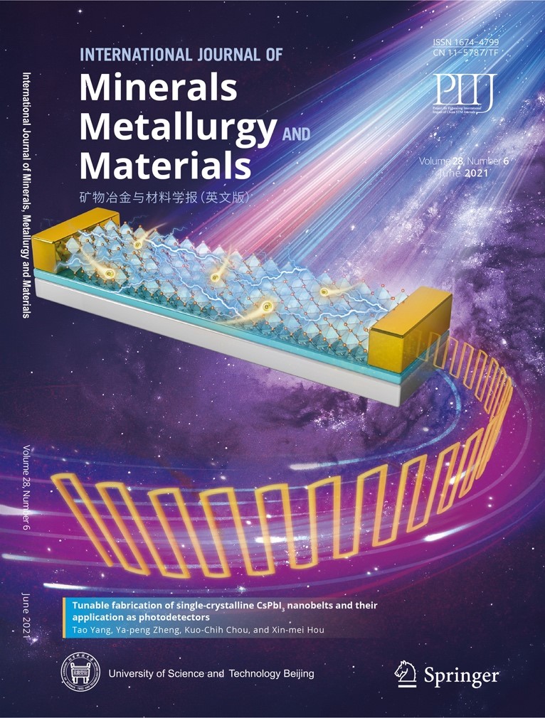
Recently, the "Green Metallurgy" research team led by Professor Hou Xinmei of University of Science and Technology Beijing published a research paper titled "Tunable fabrication of single-crystalline CsPbI3 nanobelts and their application as photodetectors", and proposed the method of use of low-dimensional all-inorganic perovskite to improve the performance of photodetector. This paper was selected as the front cover of International Journal of Minerals, Metallurgy and Materials.

Figure 1 the front cover of International Journal of Minerals, Metallurgy and Materials
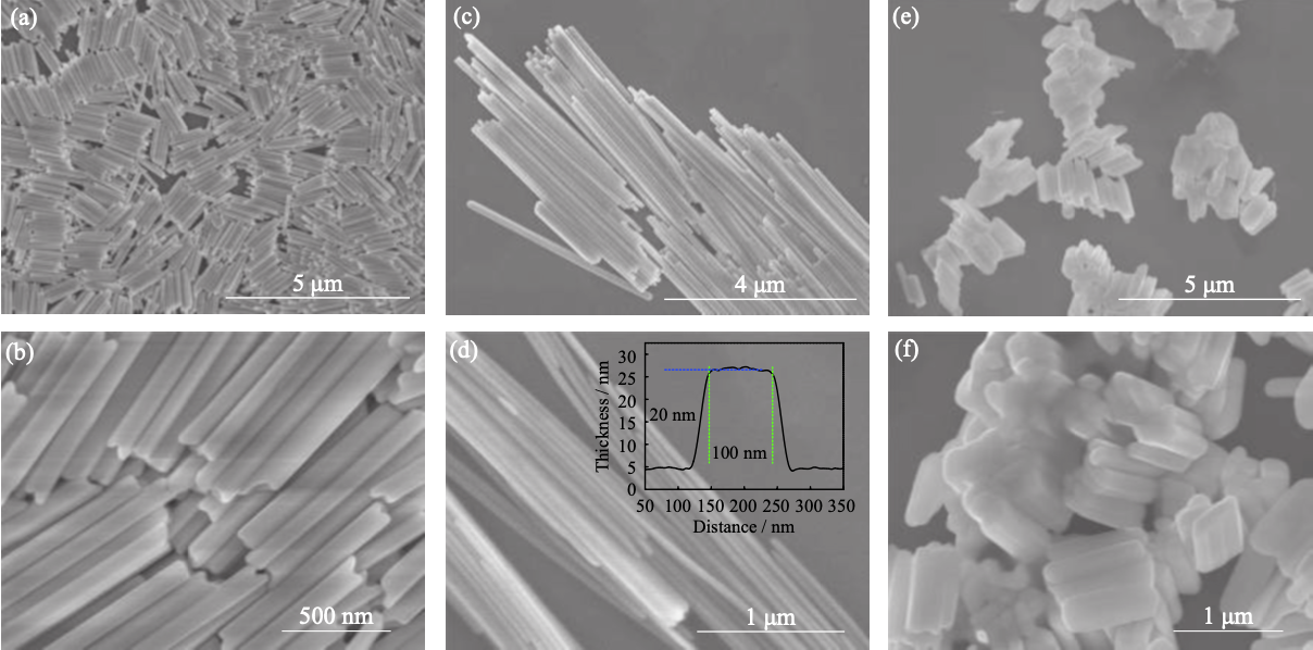
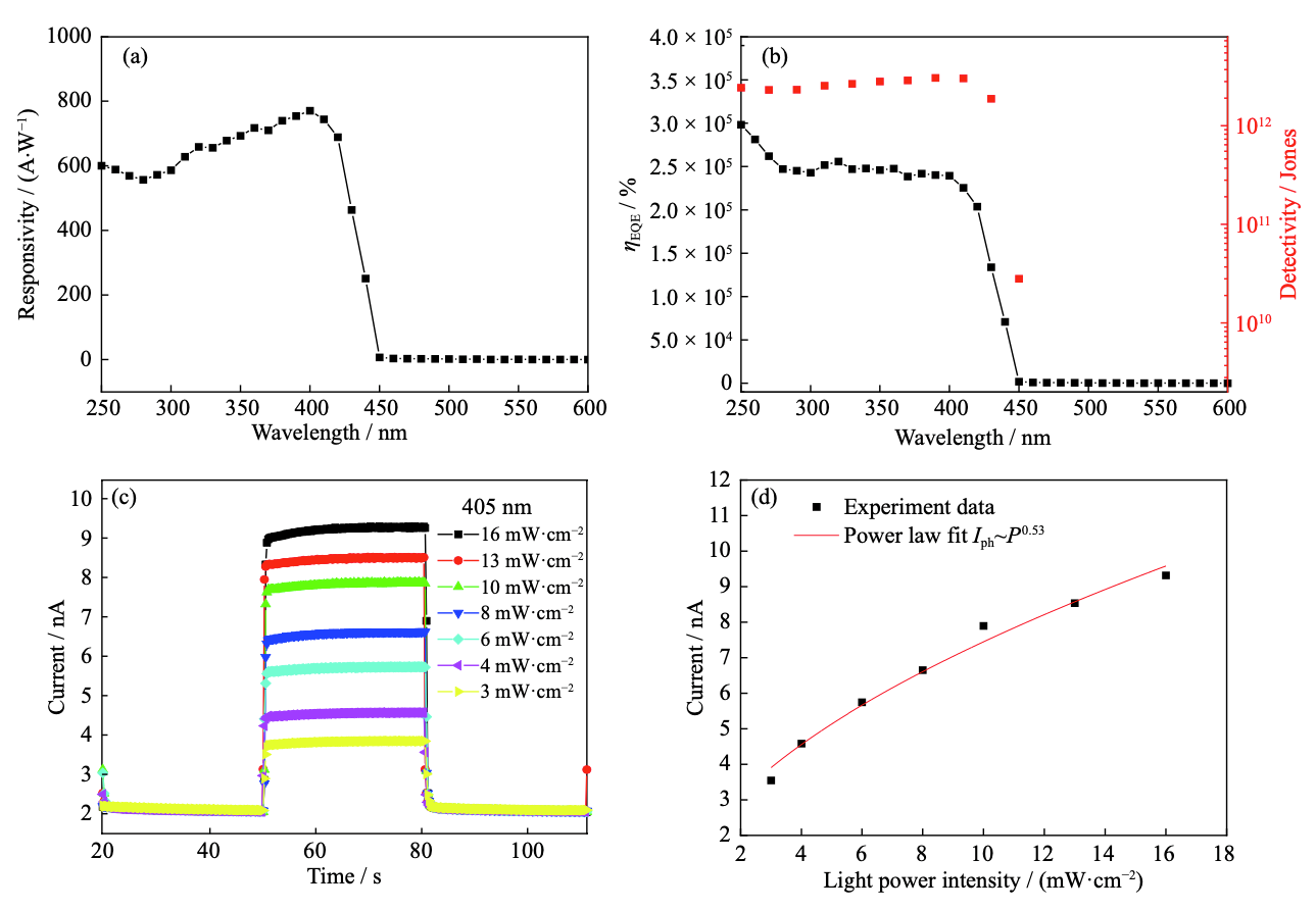
It has been reported in our recent work that the introduced PbI2 amount played a fundamental role in preparation of defect-free and high-quality one-dimensional CsPbI3 nanobelts. The microstructure of the as-prepared CsPbI3 was revealed by SEM techniques. When 96 mg PbI2 was introduced (Figure 2), the resultant product are pure nanorods with a uniform diameter of 150 nm or so and an average length of 2 µm. When 87 mg PbI2 was introduced (Figure 2c and d), the resultant products are highly purified nanobelts with a mean width, length and thickness of 100 nm, 5 µm and 20 nm, respectively. The typical width and thickness are measured to be about 100 nm and 20 nm by atomic force microscope (AFM) (the inset of Figure 2d). The width/thickness (w/t) ratio is above 5. However, when the introduced PbI2 was further up to 105 mg (Figure 2e and f), the as-synthesized nanorods began to aggregate and conglutinate. Then, the PDs based on individual CsPbI3 nanobelt were constructed and exhibited an overall good performance with a responsivity of 770 A·W-1, an external quantum efficiency of 2.39×10⁵ % and a detectivity of 3.12×10¹² Jones, which is on par with the detectivity of a Si photodetector in the same spectral region (Figure 3).
The excellent performance of perovskite nanobelt PDs is mainly attributed to following aspects. Firstly, the single-crystal CsPbI3 nanobelt has a high crystallinity, which can provide a smooth and short path for carriers transfer to enhance the response speed; Secondly, the single-crystal nanobelt have low density of defects with limited recombination of charge carriers. Thirdly, the absorption coefficient of the perovskite reaches the order of 104 cm-1, which can be ascribed to the direct bandgap nature of the electronic transition. Therefore, few hundred nanometers layer of the material can be for almost complete light absorption.

Figure 2 The typical SEM images of the obtained CsPbI3 nanocrystal with the variation of the introduced PbI2.

Figure 3 (a) Representative spectral response of the PDs with wavelengths ranging from 250 to 600 nm at a bias of 2.0 V. (b) Approximate EQE and detectivity of the PDs at different wavelengths. (c) Time-response curves of a CsPbI3 nanobelt PD irradiated at 405 nm with respect to the light intensities. (d) Relationship between the photocurrents and light intensities at a fixed incident-light wavelength of 405 nm.
The "Green Metallurgy" team of the University of Science and Technology Beijing Iron and Steel Generic Technology Collaborative Innovation Center is based on the theoretical basis of metallurgical physics and chemistry, breaking through the limitations of traditional metallurgy, chemical industry, energy, environment and materials, and exploring the effects of new materials in the fields of steel, energy and environment. enhancement. The main research directions of the echelon include: (1) interface reaction kinetics; (2) research on the boundary wettability of high-temperature solutions; (3) development of new high-temperature ceramic materials; (4) metallurgical process wastewater, waste liquid, flue gas and solid waste Governance and comprehensive utilization; (5) Development of new optoelectronic and power-electric functional materials and device construction, etc.; (6) Multi-structure control of functional materials based on electrochemical metallurgy. Currently, there are 1 National Outstanding Youth, 1 Professor, 2 Associate Researchers, and 1 Assistant Researcher. The team has undertaken more than 20 national, provincial and ministerial projects, published more than 150 SCI papers, applied for more than 30 patents, and won more than 10 provincial and ministerial awards.

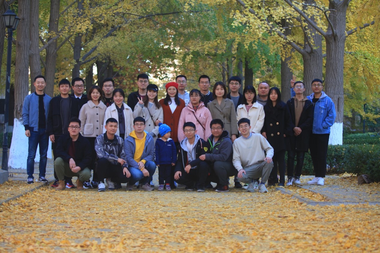
The research group of professor Xinmei Hou

The research group of professor Zhangfu Yuan

